Photonic computing has emerged as one of the most promising solutions to AI's fundamental limitations of speed and energy consumption, achieving breakthroughs in 2026 that demonstrate the viability of light-based processors for artificial intelligence. In September 2025, researchers at the University of Shanghai for Science and Technology announced an ultra-compact photonic AI chip with an under 1 mm² footprint based on Thin-Film Lithium Niobate (TFLN) technology, capable of nanosecond-scale processing. According to analysis from Ulatz, this breakthrough represents a critical inflection point as photonic computing matures to address the energy consumption crisis of conventional electronic processors, enabling sustainable AI scaling at data centers and edge deployment.
The fundamental advantage of photonic computing lies in using light instead of electricity as the information carrier, enabling computation at the speed of light with massive bandwidth through wavelength multiplexing. According to research published in Nature, photonic processors can deliver dramatic reductions in energy consumption and heat generation compared to electronic chips, with some systems demonstrating potential to surpass state-of-the-art electronic hardware by two orders of magnitude in throughput, power efficiency, and compute density. NVIDIA has recognized this potential, with Tom's Hardware reporting that the company plans to implement silicon photonics and co-packaged optics for AI GPU communication by 2026, potentially making these technologies mandatory for next-generation AI data centers.
The Physics of Light-Based Computing
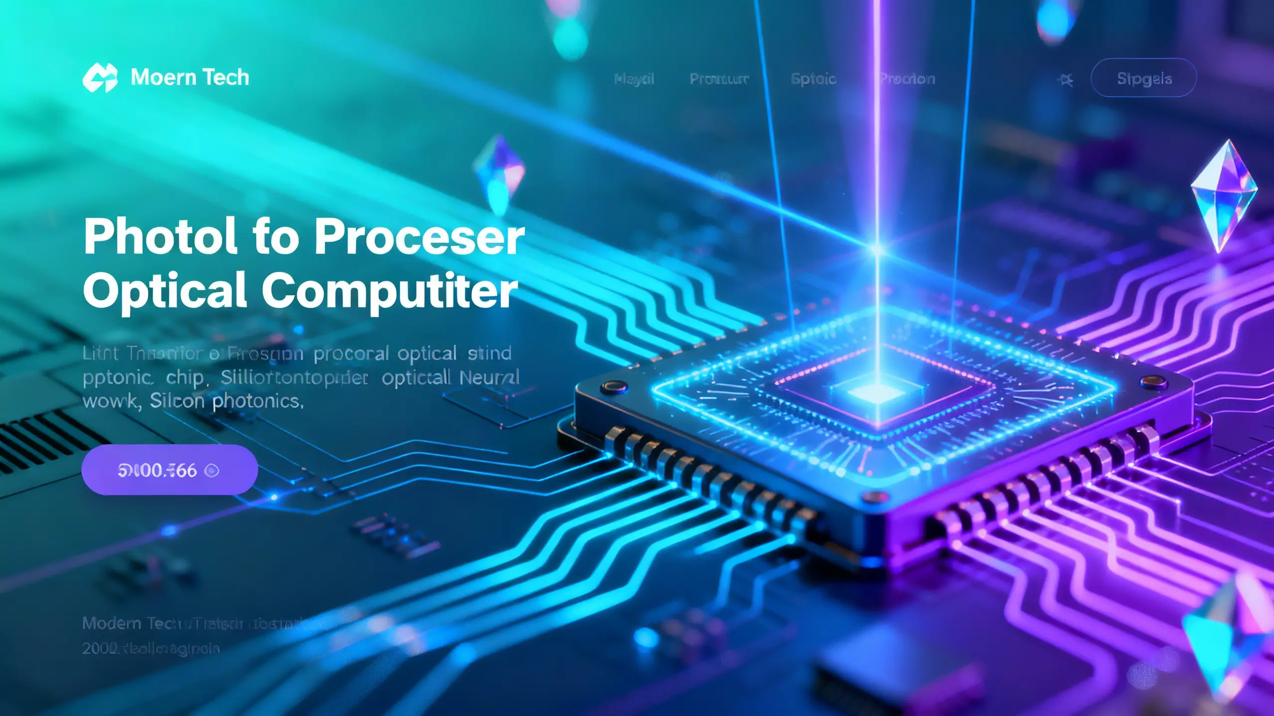
Photonic computing represents a fundamental shift from electronic to optical information processing, leveraging the unique properties of light to overcome limitations inherent in electronic systems. Unlike electrons, which experience resistance and generate heat as they move through conductors, photons travel at the speed of light with minimal energy loss and can carry information through multiple wavelengths simultaneously via wavelength division multiplexing. This enables parallel processing capabilities that far exceed what's possible with electronic circuits.
According to Nature's coverage of integrated photonic neuromorphic computing, photonic neural networks leverage coherent and incoherent optical approaches to perform linear matrix operations at exceptionally high rates and efficiency. Coherent photonic systems use interference patterns between light waves to perform computations, while incoherent systems use intensity modulation. Both approaches can achieve orders of magnitude better performance than electronic systems for specific types of operations, particularly matrix multiplications that form the core of neural network computations.
The key components of photonic processors include lasers for generating light signals, modulators for encoding information onto light waves, waveguides for routing optical signals, photodetectors for converting optical signals back to electrical signals when needed, and optical amplifiers for maintaining signal strength. Modern photonic integrated circuits (PICs) integrate these components onto silicon substrates using CMOS-compatible processes, enabling mass production and integration with electronic systems. Materials like lithium niobate offer superior performance for high-speed modulation, while silicon photonics provides cost-effective integration with existing semiconductor manufacturing infrastructure.
The September 2025 Breakthrough: Ultra-Compact Photonic AI Chips
The September 2025 announcement of an ultra-compact photonic AI chip marked a significant milestone in making photonic computing practical for real-world applications. According to detailed analysis of the breakthrough, the chip developed at the University of Shanghai for Science and Technology uses Thin-Film Lithium Niobate (TFLN) technology to achieve an under 1 mm² footprint while delivering nanosecond-scale processing capabilities. This compact size makes photonic computing viable for edge AI applications where space and power constraints are critical.
TFLN represents an advancement over bulk lithium niobate because it enables tighter integration and better performance in smaller form factors. The material's excellent electro-optic properties enable high-speed modulation of light signals, allowing the chip to process information at optical speeds. The nanosecond-scale processing capability means the chip can perform computations thousands of times faster than electronic processors for certain operations, while consuming far less energy and generating minimal heat.
The breakthrough demonstrates that photonic computing is moving from laboratory demonstrations to practical implementations. The compact form factor enables integration into mobile devices, IoT sensors, and edge computing systems where traditional electronic processors face power and thermal limitations. As photonic chip manufacturing scales and costs decrease, these ultra-compact processors may become standard components in next-generation AI systems, enabling capabilities that are impractical or impossible with electronic processors alone.
Speed and Energy Efficiency: The Photonic Advantage
The fundamental advantages of photonic computing lie in its speed and energy efficiency compared to electronic processors. According to research on photonic neural networks, optical systems can perform linear matrix operations at exceptionally high rates and efficiency, with potential to surpass state-of-the-art electronic hardware by two orders of magnitude in throughput, power efficiency, and compute density. This advantage becomes critical as AI models grow larger and energy consumption becomes a fundamental constraint.
The speed advantage stems from photons traveling at the speed of light, approximately 300,000 kilometers per second in vacuum and slightly slower in optical materials. This enables information to propagate through photonic circuits in picoseconds or nanoseconds, compared to the nanosecond to microsecond timescales of electronic circuits. For neural network computations involving massive matrix multiplications, this speed advantage compounds, enabling real-time processing of complex AI models that would require seconds or minutes on electronic processors.
Energy efficiency represents an even more critical advantage. Electronic processors consume significant power overcoming resistance in conductors and switching transistors, generating heat that requires expensive cooling systems. Photonic processors use minimal energy to generate and modulate light signals, with most energy consumed by lasers and modulators rather than signal propagation. According to analysis of photonic computing efficiency, photonic systems can achieve dramatic reductions in energy consumption for AI workloads, potentially reducing data center power consumption by orders of magnitude while enabling faster processing.
Heat generation represents another critical advantage. Electronic processors generate substantial heat that limits performance and requires expensive cooling infrastructure. Photonic processors generate minimal heat because light propagation doesn't produce the resistive heating that plagues electronic circuits. This enables higher performance densities and reduces cooling costs in data centers, making photonic computing attractive for large-scale AI infrastructure where cooling represents a significant operational expense.
Photonic Neural Networks: Scaling to Millions of Neurons
Recent breakthroughs have demonstrated that photonic neural networks can scale to handle large-scale AI applications, matching the performance of state-of-the-art deep learning models. According to research published in Science Advances, a hypermultiplexed integrated-photonics tensor optical processor demonstrated trillions of operations per second (TOPS) with 40 TOPS/W energy efficiency, using space-time-wavelength three-dimensional optical parallelism. The system, built with III/V micrometer-scale lasers and lithium niobate electro-optics, encodes data at tens of femtojoules per symbol and was verified with machine learning models of 405,000 parameters.
Even more impressive, research on large-scale optical neural networks demonstrated an optical neural network featuring over 41 million photonic neurons on a 10 mm² metasurface chip. This system matched the performance of deep learning models like ResNet and Vision Transformer on benchmark tasks, achieving speeds and energy efficiency superior to digital electronics. This represents the first demonstration that optical neural networks can handle large-scale AI applications previously thought to require electronic processors.
The scaling capability of photonic neural networks stems from wavelength division multiplexing, which enables multiple independent computations to occur simultaneously on different wavelengths of light. This parallelism enables photonic systems to process massive amounts of data in parallel, overcoming serial bottlenecks that limit electronic processors. As photonic integration improves and more wavelengths can be multiplexed, the scaling potential of photonic neural networks continues to increase, enabling systems that can handle even larger AI models with superior efficiency.
NVIDIA's Silicon Photonics Strategy: Mandatory by 2026
NVIDIA has recognized the potential of photonic computing and is planning significant integration of silicon photonics into its AI infrastructure. According to Tom's Hardware reporting, NVIDIA plans to implement silicon photonics and co-packaged optics for AI GPU communication by 2026, with these technologies potentially becoming mandatory for next-generation AI data centers. This represents a strategic shift toward optical interconnects to address bandwidth and energy limitations of electrical interconnects in large-scale AI systems.
Silicon photonics enables integration of optical components onto silicon substrates using CMOS-compatible processes, enabling cost-effective manufacturing and integration with electronic processors. Co-packaged optics places optical transceivers directly on or near processor packages, reducing the distance signals must travel and enabling higher bandwidth with lower energy consumption. For AI data centers where thousands of GPUs must communicate at high speeds, optical interconnects offer advantages in bandwidth, latency, and energy efficiency compared to electrical interconnects.
NVIDIA's adoption of silicon photonics reflects broader industry recognition that photonic technologies are becoming essential for scaling AI infrastructure. As AI models grow larger and require more computational resources, the bandwidth and energy limitations of electrical interconnects become fundamental constraints. Optical interconnects enable higher bandwidth with lower energy consumption, making them attractive for next-generation AI systems. NVIDIA's timeline suggests that photonic technologies will transition from optional enhancements to essential components of AI infrastructure within the next few years.
Single-Chip Integration and Coherent Optical Systems
Recent advances have demonstrated fully integrated photonic neural networks on single chips, representing a major step toward practical deployment. According to research published in Nature Photonics, researchers have demonstrated a fully integrated coherent optical neural network on a scalable photonic integrated circuit that monolithically integrates multiple coherent optical processor units for matrix algebra and nonlinear activation functions into a single chip. This integration enables compact, efficient photonic computing systems that can be manufactured at scale.
Coherent optical systems use interference patterns between light waves to perform computations, enabling precise control over signal processing. The integration of multiple processor units on a single chip enables parallel processing of different parts of neural networks simultaneously, improving throughput and efficiency. The monolithic integration reduces losses from coupling between components and enables more compact systems, making photonic computing practical for a wider range of applications.
The single-chip integration represents progress toward making photonic computing as accessible as electronic computing. Early photonic systems required complex optical setups with discrete components, limiting practical deployment. Modern integrated photonic circuits enable photonic computing systems that can be manufactured using semiconductor processes and integrated with electronic systems, enabling hybrid architectures that combine the strengths of both technologies. This integration is essential for making photonic computing practical for commercial deployment.
Applications: From Edge AI to Data Center Acceleration
Photonic computing enables applications across the spectrum from edge devices to data center infrastructure, each benefiting from different aspects of photonic advantages. At the edge, ultra-compact photonic chips enable AI processing in devices with strict power and size constraints, including mobile devices, IoT sensors, and autonomous systems. The energy efficiency of photonic processors extends battery life and reduces cooling requirements, enabling always-on AI capabilities that are impractical with electronic processors.
In data centers, photonic computing addresses fundamental limitations of electronic processors for AI workloads. The speed and energy efficiency advantages enable faster training and inference of large AI models while reducing power consumption and cooling costs. Optical interconnects between processors enable higher bandwidth communication, reducing bottlenecks in distributed AI training. As AI models continue to grow, photonic computing may become essential for maintaining reasonable training times and energy consumption.
Specialized applications benefit particularly from photonic computing's strengths. Real-time signal processing, image recognition, and pattern matching can leverage photonic processors' parallel processing capabilities and speed advantages. Scientific computing applications involving large matrix operations can achieve dramatic speedups with photonic processors. As photonic computing matures and becomes more widely available, new applications will emerge that leverage its unique capabilities.
Challenges: Manufacturing, Integration, and Programmability
Despite significant progress, photonic computing faces challenges on the path to mainstream adoption. Manufacturing complexity represents a major hurdle, as photonic integrated circuits require precise fabrication of optical components with nanometer-scale tolerances. While silicon photonics enables CMOS-compatible manufacturing, the processes are more complex than standard electronic fabrication, leading to higher costs and lower yields. As manufacturing processes mature and scale, costs should decrease, but photonic chips may remain more expensive than electronic chips for the foreseeable future.
Integration with electronic systems presents another challenge. Most AI systems require hybrid architectures that combine photonic processors for specific operations with electronic processors for control, memory, and other functions. Efficient integration requires careful design of interfaces between optical and electronic domains, including high-speed modulators and photodetectors. The development of better integration techniques and hybrid architectures is essential for making photonic computing practical.
Programmability represents a third challenge. Programming photonic processors requires understanding optical physics and signal processing, which differs significantly from traditional programming models. Developing software tools and frameworks that abstract away optical complexity and enable developers to program photonic systems using familiar interfaces is essential for broader adoption. Research into photonic programming models and compiler technologies is ongoing, but more work is needed to make photonic computing as accessible as electronic computing.
Material limitations also present challenges. Different materials offer different trade-offs between performance, cost, and integration capability. Silicon photonics offers cost-effective integration but limited performance for some applications. Lithium niobate offers superior performance but higher costs and more complex integration. Finding optimal materials and developing better fabrication techniques for high-performance materials is an ongoing research direction.
Future Directions: Toward General-Purpose Photonic Computing
The future of photonic computing involves expanding beyond specialized applications toward more general-purpose capabilities. Current photonic processors excel at specific operations like matrix multiplications but require electronic processors for control and other functions. Research into more complete photonic computing systems that can handle a wider range of operations is ongoing, with progress toward photonic memory, control logic, and programmability.
Hybrid architectures that combine photonic and electronic processors represent a near-term path forward, leveraging each technology where it excels. Photonic processors handle compute-intensive operations like neural network inference, while electronic processors handle control, memory access, and other operations. As photonic capabilities expand, the balance may shift toward more photonic processing, but hybrid architectures will likely remain important for the foreseeable future.
Scaling represents another future direction. Current photonic systems demonstrate impressive capabilities but operate at scales smaller than the largest electronic systems. Scaling photonic computing to handle the largest AI models will require advances in integration, manufacturing, and architecture. Research into wafer-scale photonic systems and three-dimensional integration offers paths toward larger-scale photonic computing.
New materials and technologies continue to emerge, offering potential improvements in performance, efficiency, and integration. Research into novel photonic materials, quantum photonic computing, and other advanced approaches may enable capabilities beyond current photonic systems. The field is advancing rapidly, with new breakthroughs and capabilities emerging regularly as researchers push the boundaries of light-based computing.
Conclusion: The Photonic Computing Revolution
Photonic computing has reached a critical inflection point in 2026, with ultra-compact chips, large-scale neural networks, and industry adoption demonstrating that light-based processors are ready for practical deployment. The speed and energy efficiency advantages of photonic computing address fundamental limitations of electronic processors for AI workloads, enabling sustainable scaling of AI capabilities. As manufacturing matures, costs decrease, and integration improves, photonic computing may become essential infrastructure for next-generation AI systems.
The convergence of materials science, semiconductor manufacturing, and AI development is creating unprecedented opportunities for photonic computing. Ultra-compact chips enable edge AI applications, large-scale neural networks demonstrate capability for major AI workloads, and industry adoption by companies like NVIDIA signals recognition of photonic computing's importance. The coming years will see continued scaling, improved integration, and broader adoption as photonic computing proves its value across diverse applications. For an AI industry facing speed and energy constraints, photonic computing offers a path forward that leverages the fundamental advantages of light to enable capabilities that are impractical or impossible with electronic processors alone.